Semiconductor Industry Jobs in India - The Next Big Opportunity
Semiconductor Industry Jobs in India - The Next Big Opportunity
Five years from now, I think India's chip industry will look completely different from today. Or maybe not — prediction is hard, especially about something this capital-intensive and technically demanding.
Here's what I'm fairly confident about: the money is real. The India Semiconductor Mission has Rs. 76,000 crore behind it. Micron is building a $2.75 billion facility in Gujarat. Tata Electronics is building a fabrication plant in Dholera and a packaging facility in Assam. CG Power has approval for a Rs. 7,600 crore OSAT facility in Sanand. These are not PowerPoint promises — construction is underway, engineers are being hired, and training programmes have started sending batches to facilities in the US, Japan, and Singapore.
Here's what I'm less confident about: whether India can actually build a world-class semiconductor manufacturing ecosystem from nearly zero in the timeline the government is hoping for. Taiwan took 35 years to get TSMC where it is. India is starting late and the learning curve is steep. There will be setbacks.
The career question, then, sits somewhere between certainty and uncertainty. The jobs are being created right now. The long-term trajectory is promising. But the specifics — exactly how many jobs, in which specializations, at what salary levels — involve a degree of guesswork that I want to be upfront about.
Why This Is Happening Now
The global chip shortage of 2020-2022 scared governments worldwide. When supply chain disruptions shut down automobile production, consumer electronics manufacturing, and even hospital equipment supply — all because a handful of fabs in Taiwan and South Korea couldn't meet demand — every major economy decided it needed its own chip capacity.
The US passed the CHIPS Act ($52 billion). The EU launched its Chips Act (EUR 43 billion+). Japan and South Korea announced massive incentive programmes. India, recognizing both the strategic vulnerability of importing all its chips and the economic opportunity, launched the ISM.
This isn't just industrial policy. This is geopolitical anxiety turning into capital allocation. And when that much money flows toward a sector, jobs follow.
India's Existing Strength: Design
Here's something that gets overlooked in the "India is building chip fabs" headlines: India already has roughly 20% of the world's semiconductor design engineers. Intel, Qualcomm, Texas Instruments, AMD, Broadcom, NXP, STMicroelectronics — they all have major design centres in Bangalore, Hyderabad, and Noida. Indian professionals hold senior leadership positions at nearly every major chip company globally.
What India has lacked is the manufacturing side. We design chips that get fabricated in Taiwan. That gap is what the current investment wave is trying to close.
This matters for career planning because the chip design job market in India is already mature and well-paying. The manufacturing job market is the new, uncertain, potentially massive opportunity.
The Investment Map
Micron in Sanand, Gujarat: Assembly, testing, and packaging of memory chips (DRAM and NAND flash). $2.75 billion investment, with about $1.5 billion subsidized by central and state governments. Not a fabrication plant — the silicon wafers will still be made at Micron's fabs abroad — but the packaging and testing operations are sophisticated and create thousands of engineering jobs.
Tata Electronics in Dholera, Gujarat: A semiconductor fabrication facility, in partnership with Taiwan's PSMC for technology transfer. This is the big one — India's first significant chip fab. Also building an OSAT facility in Jagiroad, Assam. Tata has been aggressively hiring experienced semiconductor professionals from Taiwan, South Korea, and the US.
CG Power (Murugappa Group) in Sanand, Gujarat: Rs. 7,600 crore OSAT facility.
Kaynes Technology in Telangana: Chip packaging facility, adding Hyderabad to the semiconductor manufacturing map.
Equipment suppliers expanding: Applied Materials, Lam Research, Tokyo Electron are growing their India operations to support the coming domestic demand.
C-DAC: Working on indigenous chip designs including the VEGA series of RISC-V processors.
Gujarat — specifically the Sanand-Dholera corridor — is becoming India's semiconductor manufacturing centre. Bangalore remains the chip design capital. Hyderabad has both design centres and incoming manufacturing. Chennai, Noida, and Assam are emerging locations.
The Jobs: What Exists Now vs. What's Coming
Chip Design (exists now, well-established)
VLSI design is the established, high-paying side of the Indian semiconductor industry. India has an estimated 150,000-200,000 people in design and related activities.
RTL Design Engineers: Write hardware description code (Verilog, SystemVerilog) that defines digital circuits. Similar to programming but the code becomes silicon. Starting salaries for M.Tech graduates from good institutions: Rs. 14-22 lakh.
Design Verification Engineers: Ensure the design works correctly before manufacturing. Verification consumes 60-70% of total design effort because a bug in silicon costs millions. Senior verification leads (8-12 years): Rs. 40-70 lakh in Bangalore.
Physical Design Engineers: Transform verified RTL into geometric layouts of transistors and wires. Floor planning, placement, clock tree synthesis, routing. Use tools like Cadence Innovus and Synopsys ICC2. Entry: Rs. 10-18 lakh. Senior: Rs. 50-80 lakh.
Analog and Mixed-Signal Designers: Design amplifiers, data converters, PLLs, power management circuits. Still a craft-based discipline that resists automation. Experienced analog leads: Rs. 50 lakh to Rs. 1.2 crore. Scarce and well-compensated.
DFT Engineers: Design test structures built into chips. Niche specialization bridging design and manufacturing.
An M.Tech in VLSI/Microelectronics from IIT Bombay, IIT Madras, IIT Delhi, IIT Kharagpur, or IIT Hyderabad is the gold standard. NIT Trichy, NIT Surathkal, NIT Warangal, NIT Calicut are strong alternatives. IIIT Hyderabad, BITS Pilani, and IISc Bangalore are also well-regarded. Fees at NITs are significantly lower, making them excellent value.
Semiconductor Manufacturing (coming, uncertain scale)
This is where the predictions get harder.
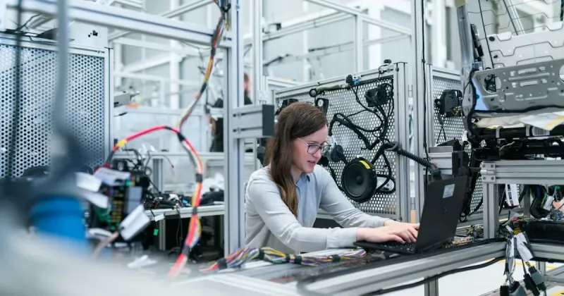
Process Engineers: Develop and refine manufacturing processes — lithography, etching, deposition, ion implantation. Work in cleanrooms wearing bunny suits. Monitor production runs, analyze data using SPC methods, troubleshoot deviations. Need deep knowledge of physics, chemistry, and materials science.
Equipment Engineers: Keep billion-dollar machines running. Preventive maintenance, breakdown response, qualification tests. Often develop deep expertise in specific machine types (ASML lithography scanners, Applied Materials CVD systems). Work in shifts for 24/7 coverage.
Yield Engineers: Analyze defects, improve manufacturing yields. Part detective work, part statistics, part materials science.
Test Engineers: Develop programmes for automated test equipment. Debug test failures, work with fab and design teams on root cause analysis.
Packaging Engineers: Design and improve chip packaging. Advanced packaging (chiplets, 3D stacking, fan-out wafer-level packaging) is becoming a major innovation area.
I think manufacturing salaries will look something like this, but I'm extrapolating from global benchmarks and early Indian hiring data: Fresh graduates: Rs. 5-10 lakh. 3-5 years experience: Rs. 10-20 lakh. 7-10 years: Rs. 22-40 lakh. Senior engineers and managers: Rs. 35-65 lakh. Fab directors: Rs. 50 lakh to Rs. 1 crore+. Shift allowances and overtime typically add 15-25% to base salary in fab operations roles.
These numbers could be higher or lower depending on demand-supply dynamics as the fabs actually start operating. If there's a severe talent shortage (likely), salaries will inflate. If government training programmes produce enough talent (possible but uncertain), they'll stabilize.
Equipment and Materials (growing with the ecosystem)
Field service engineers at companies like Applied Materials and Lam Research install, maintain, and troubleshoot fab equipment. Fresh graduate: Rs. 8-14 lakh. 3-5 years experience: Rs. 18-30 lakh. Senior engineers and support managers (10+ years): Rs. 35-60 lakh. Often includes international travel and training.
Embedded Systems and Semiconductor IP
Often overlooked. ARM, Synopsys, and Cadence operate large centres in Bangalore and Hyderabad developing reusable design blocks and EDA tools. Indian startups like InCore Semiconductors are developing RISC-V processor cores. Embedded systems engineering — software running directly on chips and microcontrollers — is a vast field driven by IoT, automotive electronics, and smart devices. Entry: Rs. 5-10 lakh. Experienced: Rs. 15-35 lakh. Senior architects: Rs. 40-70 lakh.
The Skills Gap India Needs to Close
Here's the uncomfortable truth that gets glossed over in the optimistic headlines: India doesn't currently have enough people with the right skills to staff the fabs being built. We produce plenty of engineering graduates, sure. But semiconductor manufacturing requires very specific expertise — cleanroom protocols, process integration, yield analysis, equipment maintenance at a level of precision most Indian engineering programmes don't teach. The gap between what IITs and NITs cover in their standard curriculum and what a working fab needs is real and wide.
The good news is that people have noticed. IIT Bombay, IIT Madras, IIT Delhi, and IIT Hyderabad have all expanded their VLSI design and semiconductor courses in the last couple of years. BITS Pilani has introduced specialised tracks. But design courses alone aren't enough — manufacturing is a different beast that requires hands-on training in actual fab environments, which India barely has yet. That's a chicken-and-egg problem: you need fabs to train people, and you need trained people to run fabs.
Micron has been addressing this by sending batches of Indian engineers to its facilities in the US, Japan, and Singapore for months-long immersive training programmes. Tata Electronics has similar arrangements with PSMC in Taiwan. Texas Instruments, which has had design centres in India for decades, is expanding its campus hiring and running semiconductor training programmes at partner institutions. These company-led training efforts probably matter more in the short term than any curriculum change, because they're teaching people on actual equipment with actual production standards.
And then there's the experienced hire question. India is actively recruiting semiconductor professionals from Taiwan, South Korea, and the US — people who've spent 15 or 20 years running fab operations at TSMC, Samsung, or Intel. These hires are expensive, but they're the ones who'll train the first generation of Indian fab engineers. Without them, you're basically asking people to learn from textbooks how to run a billion-dollar facility. That doesn't work in this industry. The tacit knowledge — the things that aren't written in any manual — can only transfer person to person. Whether India can attract enough of these experienced professionals, and retain them long enough to build local expertise, is probably the single biggest factor that'll determine how fast the skills gap closes.
The Chips to Startup (C2S) Programme
This is worth knowing about if you're a student. MeitY's C2S programme provides over 100 Indian academic institutions with access to professional-grade EDA tools from Cadence, Synopsys, and Siemens EDA. These tools normally cost lakhs per year per licence. The programme also provides Process Design Kits and has enabled actual tape-outs — Indian students designing chips that were manufactured into working silicon.
Bold prediction: the C2S programme will produce India's first generation of semiconductor entrepreneurs. Students who've actually taped out a chip design in college have a completely different understanding of the industry than those who only studied theory.
If your institution is part of C2S, engage with it seriously. If it's not, ask why.
The India vs. World Comparison
Globally, semiconductors employ about 2 million people directly and 10 million indirectly. Taiwan alone has 300,000+ in manufacturing. India currently has nearly zero in manufacturing — all 150,000-200,000 are in design.
Industry estimates suggest 300,000-500,000 new direct manufacturing jobs in India over the next decade, with multiplier effects creating several times that number in ancillary roles.
On salary purchasing power: a process engineer earning Rs. 25 lakh in Gujarat lives comparably to one earning $90,000 in the San Francisco Bay Area, where housing alone eats most of the salary. This purchasing power gap is why some Indian semiconductor professionals who emigrated are now looking at returning.
Where India lags badly: process technology maturity. TSMC manufactures at 3-nanometre, pushing toward 2nm. India's first fabs will operate at 28nm, roughly two decades behind the leading edge. But — and this is important — the 28nm and 40nm nodes are the workhorses of the industry. Automotive chips, industrial controllers, IoT devices, power management circuits. The market for mature-node chips is massive and growing. India doesn't need to compete at the bleeding edge to build a commercially viable semiconductor industry.
My Predictions (With Appropriate Humility)
Near term (now to 2028): OSAT facilities from Micron, CG Power, and Tata (Assam) become the primary job generators. Thousands of packaging engineers, test engineers, quality professionals, and production managers. This is the window to enter manufacturing at the ground level.
Medium term (2028-2032): Tata's Dholera fab becomes operational. India's genuine entry into chip fabrication. Demand for process engineers, yield engineers, cleanroom technicians. People who gained OSAT experience in the earlier phase will be positioned to transition into fab roles.
Longer term (beyond 2032): If the initial fabs demonstrate reliable operations and competitive yields, additional investments follow. India could host 5-8 manufacturing facilities by 2035. Compound semiconductors (GaN, SiC) for power electronics and EVs become a possible Indian specialty given the country's EV and renewable energy growth.
I'm fairly confident about the near-term prediction. The medium-term one depends on Tata's execution and whether PSMC's technology transfer works well. The longer-term one is genuinely speculative.
The Honest Challenges
Water: Fabs consume millions of litres of ultra-pure water daily. Ensuring reliable supply in water-stressed India is a real problem that needs engineering solutions, not just policy statements.
Power: Even a momentary fluctuation can destroy an entire batch of wafers worth crores. India's grid has improved but semiconductor-grade power reliability is exceptionally demanding. This is partly why Gujarat (relatively good power infrastructure) is the preferred location.
Talent gap: India produces many engineering graduates, but what Indian colleges teach and what semiconductor fabs require are different things. Bridging this gap takes time. Micron has been sending Indian engineers to US, Japan, and Singapore facilities for months of immersive training. That works for the first few hundred people. Scaling to tens of thousands requires domestic training infrastructure that doesn't fully exist yet.
Execution risk: Building fabs is extraordinarily difficult. The Vedanta-Foxconn partnership faced challenges and restructuring. Not every announced project will succeed. Some delays are inevitable.
Global Demand Drivers
AI chips. Electric vehicles (an EV contains roughly twice the semiconductor content of a conventional car). 5G expansion. IoT device proliferation. Data centre growth driven by cloud and AI workloads. The AI chip market alone is projected at over $80 billion by 2028. Automotive semiconductors are expected to grow from $50 billion to over $120 billion by 2030.
This demand is structural and enduring. Semiconductor skills are globally portable. An engineer trained in India can work in Taiwan, South Korea, the US, Singapore, or Europe. The specifics of chip technology will evolve, but the fundamental importance of semiconductors to the global economy is not in question.
Getting In — Based on Where You Are
Students choosing a specialization: M.Tech in VLSI Design or Microelectronics from IIT Bombay, IIT Madras, or equivalent is the highest-ROI educational investment in this field. Starting packages of Rs. 12-25 lakh, ceiling well above Rs. 1 crore for senior specialists. Maven Silicon and Sandeepani in Bangalore offer 6-12 month VLSI programmes for working professionals or those from non-top-tier colleges.
Working professionals in IT services: Transition is possible but requires targeted upskilling. VLSI certification courses, NPTEL courses on semiconductor physics, building personal projects that demonstrate understanding. The demand-supply gap means companies are willing to invest in training people who show genuine aptitude.
Fresh engineering graduates (any discipline): The OSAT facilities opening in Gujarat and Assam will be the largest hiring sources in the near term. Mechanical, chemical, materials science, and electrical engineering backgrounds are all relevant for manufacturing roles. Apply directly to Micron India, Tata Electronics, and CG Power.
Defence and space semiconductor applications: ISRO and DRDO have long imported chips for their missions. Domestic fabrication creates potential for radiation-hardened and military-grade semiconductors. Specialized, lucrative, and serving national security objectives.
Five years from now, we'll know whether India's semiconductor push became a genuine industry or an expensive experiment. The indicators right now — the capital committed, the global demand tailwinds, the existing design talent base — point toward success. But nobody who's honest about industrial development would guarantee it.
I guess we'll find out.

Rajesh Kumar
Senior Career Counselor
Rajesh Kumar is a career counselor and job market analyst with over 8 years of experience helping job seekers across India find meaningful employment. He specializes in government job preparation, interview strategies, and career guidance for freshers and experienced professionals alike.


Comments
Be the first to leave a comment on this article.
Leave a Comment